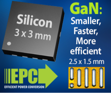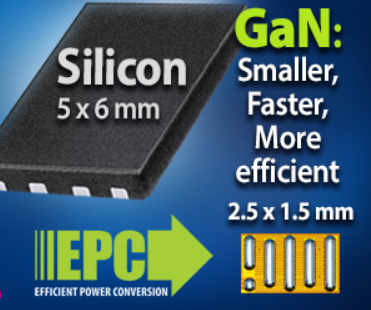

The objective of this cross-reference tool is to help you find the best GaN FETs to fit your design needs.
Data is for reference only, for design support contact us via GaN Talk Support Forum EPC

Back to the cross reference page
Data is for reference only, for design support contact us via GaN Talk Support Forum EPC
Back to the cross reference page

| Part Comparison Summary: | ||||||||||
| FET Operating Conditions | ||||||||||
| Part Number | PSMN1R0-40YSH (Nexperia) | EPC2302 X | EPC2067 X | EPC2066 X | EPC2206 X | EPC2071 X | ||||
| Modify EPC Part | ||||||||||
| BVDSS [V] | 40.0 | 100.0 | 40.0 | 40.0 | 80.0 | 100.0 | ||||
| RDS(ON) [mΩ] [Typ] | 1.69 | 1.40 | 1.30 | 0.80 | 1.80 | 1.70 | ||||
| RTHJC [°K/W] | 0.45 | 0.20 | 0.40 | - | 0.40 | - | ||||
| QG Typ [nC] | 42.0 | 23.0 | 17.1 | 25.0 | 15.0 | 18.0 | ||||
| Gate Drive [V] | 10.0 | 5.00 | 5.00 | 5.00 | 5.00 | 5.00 | ||||
| Gate Drive Loss [W] | 0.010 | 0.0028 | 0.0021 | 0.0030 | 0.0018 | 0.0022 | ||||
| Package Area [mm2] |
W=5.13mm, L=6.05mm
Area=31.0 mm2 |
W=3.00mm, L=5.00mm
Area=15.0 mm2 |
W=2.85mm, L=3.25mm
Area=9.3 mm2 |
W=2.30mm, L=6.05mm
Area=13.9 mm2 |
W=2.30mm, L=6.05mm
Area=13.9 mm2 |
W=2.30mm, L=4.45mm
Area=10.2 mm2 |
||||
| Calculated Total Power Loss [W] | 0.12 |
0.097 |
0.094 |
0.086 |
0.12 |
0.11 |
||||
| Auto Qualified | No | No | No | No | Yes | No | ||||
| Status | Promotion | Preferred | Preferred | Preferred | Preferred | Preferred | ||||
Powered By DiscoverEE - The Cross-Referencing Platform.
Visit us at www.discoveree.io
Visit us at www.discoveree.io
| Detail Power Loss Calculations: | ||||||||||
| Parameter | Value Type | PSMN1R0-40YSH (Nexperia) |
EPC2302 | EPC2067 | EPC2066 | EPC2206 | EPC2071 | |||
| Detail Parts Specifications | ||||||||||
| Click Here To See More Parameters >> | ||||||||||
| Package By Manufacturer | SOT1023 | QFN 3x5 | BARE DIE 3.25 x 2.85 | BARE DIE (6.05 x 2.3) | LGA 6.05 x 2.3 | BARE DIE(4.45 x 2.3) | ||||
| Package Mounting | SMD | SMD | SMD | DIE | DIE | DIE | ||||
| Material | Silicon | Gallium Nitride | Gallium Nitride | Gallium Nitride | Gallium Nitride | Gallium Nitride | ||||
| Configuration | Single | Single | Single | Single | Single | Single | ||||
| Auto Qualified | No | No | No | No | Yes | No | ||||
| VGS [V] | Max | -20.0, 20.0 | -, - | -, - | -, - | -4.00, 6.00 | -, - | |||
| BVDSS [V] | Max | 40 | 100 | 40 | 40 | 80 | 100 | |||
| VTH [V] | Min,Typ,Max | 2.40, 3.00, 3.60 | 0.80, 1.30, 2.50 | 0.70, 1.00, 2.50 | 0.70, 1.20, 2.50 | 0.70, 1.20, 2.50 | 0.70, 1.30, 2.50 | |||
| RDS(ON) [mΩ] | Typ,Max |
-, - |
1.40, 1.80 AT VGS = 5V ID = 50A TJ = 25C |
1.30, 1.55 AT VGS = 5V ID = 37A TJ = 25C |
0.80, 1.10 AT VGS = 5V ID = 50A TJ = 25C |
1.80, 2.20 AT VGS = 5V ID = 29A TJ = 25C |
1.70, 2.20 AT VGS = 5V ID = 30A TJ = 25C |
|||
| QG [nC] | Typ,Max | 42.0, - AT VGS = 10V |
23.0, 29.0 AT VGS = 5V ID = 50A |
17.1, 22.3 AT VGS = 5V ID = 37A |
25.0, 33.0 AT VGS = 5V ID = 50A |
15.0, 19.0 AT VGS = 5V ID = 29A |
18.0, 26.0 AT VGS = 5V ID = 30A |
|||
| QGS [nC] | Typ | 26.0 | 8.90 | 5.30 | 8.90 | 4.10 | 6.00 | |||
| QGD [nC] | Typ | 13.0 | 2.30 | 2.00 | 3.20 | 3.00 | 1.80 | |||
| CISS [pF] | Typ | 6,738.0 | 3,200.0 | 2,178.0 | 3,539.0 | 1,610.0 | 2,664.0 | |||
| COSS [pF] | Typ | 1,767.0 | 1,000.0 | 1,071.0 | 1,670.0 | 1,100.0 | 878.0 | |||
| CRSS [pF] | Typ | 310.0 | 7.00 | 24.0 | 30.0 | 15.0 | 5.40 | |||
| VSD [V] | Typ,Max | 0.77, 1.20 | 1.50, - | 1.20, - | 1.50, - | 1.50, - | 1.50, - | |||
| TRR [ns] | Typ | 45.0 | 0 | 0 | 0 | 0 | 0 | |||
| QRR [nC] | Typ | 53.0 | 0 | 0 | 0 | 0 | 0 | |||
| RG Internal [Ohm] | Typ | 1.20 | 0.50 | 0.40 | 0.40 | 0.30 | 0.30 | |||
| RTHJC [°K/W] | Max | 0.45 | 0.20 | 0.40 | - | 0.40 | - | |||
| RTHJA [°K/W] | Max | 42.0 | 45.0 | 48.0 | 51.0 | 42.0 | 59.0 | |||
| ID [A] | Typ |
290.0 AT VGS = 10V TA = 25C |
101.0 AT TA = 25C |
69.0 AT TA = 25C |
90.0 |
90.0 |
64.0 |
|||
| ID [A] | Typ |
277.0 AT VGS = 10V TA = 25C |
- |
- |
- |
- |
- |
|||
| ID(pulse) [A] | Typ | 1,564.0 | 408.0 | 409.0 | 639.0 | 390.0 | 350.0 | |||
| PD [W] | Typ |
333.0 |
- |
- |
- |
- |
- |
|||
| Figure of Merit | ||||||||||
| Gate Drive [V] | 10.0 | 5.00 | 5.00 | 5.00 | 5.00 | 5.00 | ||||
| RDS(ON)*QG [mΩ*nC] | Typ,Max | -, - | 32, 52 | 22, 35 | 20, 36 | 27, 42 | 31, 57 | |||
| RDS(ON)*COSS [mΩ*pF] | Typ,Max | -, - | 1400, 2160 | 1392, 2491 | 1336, 2111 | 1980, 3630 | 1493, 2147 | |||
| Calculated Values For Current & Power Rating | ||||||||||
| ID [A] Calc. @RTHJA max (Datasheet) | TJ=150°C, TA=25°C | 26.0 | 27.8 | 29.0 | 33.4 | 26.0 | 21.9 | |||
| ID [A] Calc. @ RTHCA=°C/W | TJ=150°C, TA=25°C | 72.2 | 81.7 | 86.4 | 106.6 | 72.5 | 75.4 | |||
| ID [A] Calc. @RTHJC max (Datasheet) | TJ=150°C, TC=25°C | 251.3 | 416.7 | 317.5 | - | 266.5 | - | |||
| PD [W] Calc. @RTHJA max | TJ=150°C, TA=25°C | 2.98 | 2.78 | 2.60 | 2.45 | 2.98 | 2.12 | |||
| PD [W] Calc. @ System | RTHJA=5°C/W, TJ=150°C, TA=25°C | 22.9 | 24.0 | 23.1 | 25.0 | 23.1 | 25.0 | |||
| PD [W] Calc. @RTHJC max | TJ=150°C, TC=25°C | 277.8 | 625.0 | 312.5 | - | 312.5 | - | |||
| Calculated Switching Turn-On and Turn-Off Times | ||||||||||
| FET Operating Conditions | ||||||||||
| td(on) [ns] | Typ | 9.61 |
3.73 |
1.81 |
3.71 |
1.69 |
3.11 |
|||
| tr [ns] | Typ | 5.31 |
1.65 |
1.21 |
2.16 |
2.03 |
1.29 |
|||
| td(off) [ns] | Typ | 9.07 |
5.23 |
4.70 |
6.35 |
2.89 |
4.35 |
|||
| tf [ns] | Typ | 5.10 |
2.08 |
2.35 |
3.14 |
2.94 |
1.63 |
|||
| Calculated Power Loss | ||||||||||
| Gate Drive [V] | 10.0 | 5.00 | 5.00 | 5.00 | 5.00 | 5.00 | ||||
| Gate Drive Loss [W] | 0.010 | 0.0028 | 0.0021 | 0.0030 | 0.0018 | 0.0022 | ||||
| RDS(ON) [mΩ] at TJ | Typ | 0 @26.2°C |
1.2 @25.6°C |
1.3 @25.6°C |
0.8 @25.5°C |
1.8 @25.8°C |
1.7 @25.7°C |
|||
| Calculated Conduction Loss [W] | Typ | - |
0.061 |
0.065 |
0.040 |
0.090 |
0.085 |
|||
| Calculated Switching Loss [W] | Max | 0.064 |
0.026 |
0.019 |
0.031 |
0.022 |
0.021 |
|||
| Diode Reverse Recovery Power Loss [W] 1 | Typ | 0.030528 |
||||||||
| Output Capacitor Power Loss [W] | Typ | 0.012 |
0.0069 |
0.0074 |
0.012 |
0.0076 |
0.0061 |
|||
| Calculated Total Power Loss [W] | Typ | 0.12 |
0.097 |
0.094 |
0.086 |
0.12 |
0.11 |
|||
| Estimated TJ at RTHCA=5°C/W [°C] | Typ | 26.2 | 25.6 | 25.6 | 25.5 | 25.8 | 25.7 | |||
| Rated Junction Temperature [°C] | Max | 175.0 | 150.0 | 150.0 | 150.0 | 150.0 | 150.0 | |||
1: Reverse Recovery losses are calculated from default datasheet conditions and these losses can be much higher in actual operating conditions.

